PCB design | Circuit board design | PCB Design for IoT Plant
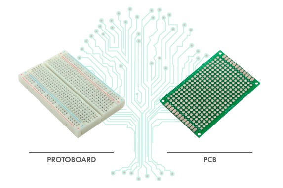
Always when starting the journey to the maker world, one of the first things that you have to learn is to understand and design circuits. After all, only then can we bring our ideas to life and interact with the “real world”, right? And, In this context, one of the first things we have contact with is the protoboard, a platform for prototyping very useful and versatile hardware. So in this article I will discuss with details about PCB design or circuit board design, However, the protoboard leaves something to be desired when it comes to the application of circuits in more hostile environments and real applications / outside our laboratories, that is, when things are more serious and more consolidated the prototype is required. Therefore, the next step in a project (after being validated on a protoboard, of course) is to have a PCI - PrintedCircuit Board (or,, PCB: Printed Circuit Board ), so you can go out into the field without fear (and, in addition, give your project a more professional look).
 |
| Circuit board design |
And this is
exactly what this series of posts will teach you: how to assemble your own printed
circuit boards, based on our Planta IoT project. That's right: the IoT
Plant project will have its own board and the best: everything is free for you
to edit and make any changes you want! You can also choose to use already
perforated plates, such as perforated phenolite or double-sided perforated
plates , available at the FILIPEFLOP store.
Printed Circuit Boards - what are they?
If you are just
starting out in the maker world, this may be a natural issue at this point in
this post. In a very simplistic way, a printed circuit board or PCB can be
defined as a piece of rigid insulating material (usually phenolite or
fiberglass, generally rectangular in shape) that contains layers of circuits
designed in conductive material (copper), thus forming a “circuit
sandwich”. On the bottom and top surfaces of this board, the electronic
components used in the circuit in question are welded.
As an example,
there are all the “little signs” that we have, including Arduinos. Each
layer of conductive material / circuit is called a Layer, the more complex the
circuit, the more Layers will be needed to make your Printed Circuit Board.
Multi-colored
Printed Circuit Boards
In addition, in
summary, there are other important elements in Printed Circuit Boards:
- Mask
/ Silk : they make it possible to color the Printed Circuit
Boards (in blue, green, black, white, red, etc.) and place inscriptions on
them. This is a very important layer, both aesthetically and in terms
of information about the circuit to be assembled (component codes, values,
polarization, etc.).
- Holes layer :
this is a “layer” used in the development of Printed Circuit Boards that
contains information about each hole to be made in the board, from the
positioning and diameter of each hole to the amount of conductive material
to be placed on the board. around each hole.
Making a simple
analogy:
- Instead of
protoboards, there are copper surfaces (layers, or Layers )
- Instead of
points for connecting the components, you have the holes of a PCB
- Instead of
wires and jumpers, there are the tracks of a printed circuit.
It is also
important to note that not all PCB factories have the same manufacturing
technologies. That is, the more complex (more Layers, shorter trails,
smaller holes, etc.) a board is, the more restricted the range of manufacturer
options is (and the more expensive it is to manufacture, as a result).
What to use to create a PCB design or circuit board design?
Nowadays,
luckily there is several software available for this task, being both paid and
extremely powerful software as well as free and open-source software. PCB design or circuit board design is to cite some examples, we have:
- Eagle
- Altium
- Proteus
PCB Designer
- ZenitPCB
- KiCad EDA
For our series
of posts and development of PlantaIoT Board, the KiCad EDA software was chosen
(called in the articles only KiCad). The main reasons for the choice are:
it is free, open-source, multi-platform software (runs on Linux, Windows and OS
X), user-friendly interface and widely used by the community (there are many
tutorials on the Internet, including in Portuguese , which facilitates
learning). Experienced readers will immediately remember the homesick
Eagle (one of the only free options with possible limitations a few years ago)
when using KiCad.
Note: if you, like me, use Ubuntu (in
my case, version 16.04 LTS), KiCad is already included as one of the packages
in the standard repositories. This means that you can download it directly
from the terminal.
What is possible to do with KiCad?
The answer is
simple: all stages of PCB development. In other words, this tool allows
you to develop your PCB from the design of the schematic circuit to the
generation of Gerber Files (we'll see what that is in detail throughout the
series, don't worry). In summary, there are four steps to follow to
develop a PCB:
- Schematic
circuit drawing.
- Relationship
of the components used with your footprint. That is, correspondence
between each component used and the way it will be drawn on the PCB.
- PCB design
and routing (trail design procedure).
- Generation
of Gerber Files (files used by PCB manufacturers to manufacture them)
It is worth
mentioning that KiCad does not do circuit
simulations. So, before you start designing your project's PCB,
be absolutely sure that it works (do simulations, assemble your
project on the protoboard beforehand and validate it).
Opening KiCad for the first time
After
installing KiCad, when you open it you will see a screen with a blank project
tab. Observe the following figure:
 |
| PCB design |
KiCad software opened for the first
time
To start /
create a new project, click File > New Project > New
Project . After naming your project and choosing where it should
be saved, your screen will be as shown in the image below. In blue, the
.sch file stands out, corresponding to the file that will contain the schematic
circuit design of your project.
 |
| Circuit board design |
Creating a project in the KiCad
software
IMPORTANT: Save the project to a known
folder / that you have easy access to. If you save anywhere and don't care
about it too much, you will have trouble backing up your project and copying
the Gerber Files.
KiCad usage tips
For a better
use of the tool, I leave the following tips:
- Use it
with two monitors (or a large monitor), as there will be times when it
will be necessary to consult different information on different screens at
the same time.
- Have (a
lot) patience. Designing a PCB from the schematic to having the
gerber files is a lengthy and detailed procedure (especially for those
starting out), where an error can ruin an entire batch of manufactured
PCBs. Therefore, if your project requires a PCB, set aside special
development time for this, preferably in environments where you will not
experience many interruptions.
- Be aware
that (very) hardly a manufacturer will make a part just for you to
test. There is usually a minimum batch that manufacturers impose
(this varies from manufacturer to manufacturer). Therefore, review
the schematic circuit and PCB several times (if possible, ask other people
to review it as well) before ordering fabrication, so the loss of material
(and money) is minimized.
- How to
modify a PCB after its manufacture is not so simple (and extremely not
recommended), if possible, try to leave all possibilities open in the
schematic circuit and in your PCB. For example, if you are going to
use a microcontroller and, from it, use only a few GPIOs / pins, leave the
signals from the other pins available in pin bars (or even islands).
This is interesting because you rarely know all the directions that your project will take and, in case there is a need for expansion of functionalities, it may not be necessary to modify the PCB (= reduction in the final cost of the project). - Avoid
using any software for PCB development in virtual machines. This
software requires some processing and a good amount of RAM, making its use
inappropriate in virtual machines.
- Before
actually developing a PCB, have a list of manufacturers (national and
international) and, at the end of the development, make a budget with most
of them. This list you can go riding with time and need for more
suppliers.
Next step: schematic circuit design
You will be
shown how to draw schematic circuits in KiCad and the schematic circuit design
of the IoT Board Plant. Don't miss the next post!!
PCB Design or circuit board design for IoT Plant
Now, let's go
ahead with the IoT Plant PCB project! Check out the first part of
this series of posts , which show how to make the printed circuit board
for the IoT Plant project shown here on the FILIPEFLOP blog! In
this second post, I will show you how to install a
library of ESP8266 components on the KiCad and how to make the schematic
circuit of the PCB of the IoT Plant. Get to work!
Schematic PCB circuit
Before
starting your schematic circuit design, you must have the schematic of the
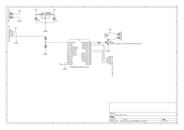
circuit in hand (to know what will be drawn). Therefore, below is a figure
with the schematic circuit of the IoT Plant:
 |
| Circuit board design |
Bill of Materials
In
the circuit design, the components of the list / Bill Of Materials (BOM)
below will be used:
- Two
connectors with 2-terminal screws (on KiCad, they are called
Screw_Terminal_1x02)
- TO-220
encapsulation regulator 7805 (on KiCad, it is called LM7805CT)
- NodeMCU
Wifi ESP8266
- Two
4-terminal female connector bars (on KiCad, they are called CONN_01x04) *
- Resistor
of 100Ohm 1 / 4W . In KiCad, it is simply called a Resistor.
- 200Ohm 1 / 4W resistor . In KiCad, it is simply called a
Resistor.
- Two
electrolytic capacitors (also called polarized capacitors). In KiCad,
they are called Polarized Capacitor.
- Diode
1N4007 **
- BC337
Transistor ***
Legend:
* Although necessary to assemble the circuit and PCB, it is not necessary (it
is recommended, but it is not necessary) to buy this (these) component (s).
Reason: it is possible to weld the wires on the generated islands.
** KiCad does not have this diode by default, but you can use the KiCad
“generic” diode (called Diode only) to design the circuit
*** KiCad does not have this transistor by default. Therefore, you can use
its equivalent, BC817 (both have the same physical dimensions and operating
characteristics, so you can, when assembling the PCB, use BC337 or BC817).
Important:
it is
highly recommended to place a heatsink on the voltage regulator (7805).
Creating the project and opening the
schematic circuit file
First,
you need to create the PlantaIoTBoard project . To
do this, as shown in the topic “Opening KiCad for the first time”, create the
project. After that, double click / open the project's .sch file . You
should then see the schematic circuit file with nothing drawn, as shown in the
following figure:
 |
| Circuit board design |
Screen that will contain the schematic
circuit design of PlantaIoT Board
Now,
everything is ready for the schematic circuit design!
ESP8266 libraries - installation
Before
proceeding with the circuit design, it is necessary to install a component
library from the ESP8266 line. This is necessary because, unfortunately,
these components do not come by default with KiCad, but the good news is that
it is quite easy to get and install them (I found a good library for
ESP8266 in
this GitHub repository ). To install the library, follow the
procedure below.
Note: the procedures
described focus on Linux, but it is easily done on Windows with similar
actions.
- First,
make a clone of the repository on your computer (in a known / easily
accessible location)
In Linux, through the terminal, execute the following commands:
?
|
1 two 3 4 |
cd ~ mkdir -p ~/kicad/libraries/ cd ~/kicad/libraries/ git clone https://github.com/jdunmire/kicad-ESP8266 |
- On the
schematic circuit screen, go to the Preferences > Component
Libraries > Add menu and add the
ESP8266.lib file (which you downloaded when you cloned the repository).
- To add the
footprints of the components: on the main KiCad screen, open the file with
the name ending in “_pcb”, access the Preferences menu > Footprint
Libraries Wizard and add the file ESP8266.pretty (contained
where you cloned the repository).
That
done, KiCad will be ready for you to be able to design schematic and PCI
circuits for the project.
Placing the circuit components in the
schematic
To
place a component in the schematic circuit, follow the procedure below:
- Go
to Place > Component
- Click on
the "sheet" location of the schematic circuit where you want to
add a component
- The
following window will appear:
 |
| Circuit board design |
- Navigate
through it (or type the name of the desired component in Filter:, select
the desired component and click OK.
- Once this
is done, the window will close and it will be possible to position the
component on the “sheet”. To confirm the location of the component,
click on it with the left mouse button.
- If you
want to rotate the component, press the Esc key, right-click on it and
click Orient Component. Rotate it as desired.
Do
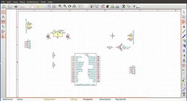
this procedure for all components of the circuit (according to the list of
components shown in this post). Your schematic circuit should look similar
to the figure below:
 |
| Circuit board design |
Naming the components
You
may have noticed that the components are unnamed "formal" (resistors
called "R?", Capacitors called "C?", Etc.). KiCad has
a feature to automatically name the components of a schematic
circuit. Such functionality is called Annotate schematic
components . to access it, just go to Tools > Annotate
Schematic .
Going
to this option, a window will appear. Click on Annotate and
all components are automatically named. Observe the following figure:
 |
| PCB design |
Connecting the components
To
connect the components, we will use wires . To place a
wire between a terminal of one component and another element (terminal of
another component, for example). follow the procedure below.
Tip: For this task, the use of zoom is recommended. To
zoom in, roll the mouse scroll up and, to zoom out, roll the mouse scroll down.
- Go
to Place > Wire
- Click on
the terminal of a component you want to join to another element
- Move the
mouse to the target element to be joined by the wire (terminal of another
component, for example). Click on it once.
Do
this procedure until the circuit has the connections identical to the complete
schematic of the PlantaIoT Board provided here (at the beginning of this post).
Using Power Ports for PCB design or circuit
board design
Power Ports are elements that
represent power (+ 12V, + 5V, GND, etc.), as shown in the image below:
 |
| PCB design |
These
elements are very useful as they make the schematic circuit cleaner and more
understandable (especially for large circuits). To add them, follow the
procedure below:
Go
to Place > Power Port
Click
on the "sheet" location of the schematic circuit where you want to
add a Power port
The
following window will appear:
 |
| PCB design for IoT |
- Navigate
through the “power” options and place the + 12V, + 5V and GNDREF power
ports according to the complete schematic circuit provided in the
article. At the end of this process, your schematic circuit should
look similar to the figure below:
 |
| PCB design MAD PCB |
Schematic ready!
At
this point, your schematic circuit of the IoT Board Plant is ready!
Next
steps: generate the PCB and gerber files (both will be seen in
part 3 of this series).
PCB Design for IoT Plant PCB Designor circuit board
design
Concluding
the series of posts on the IoT Board Plant, let's see how a PCB is made and
what is needed to send it for manufacturing. Check out the first and second parts of this
series, which show the fundamentals and tools for PCB projects!
In
summary, in this third and last post of the series, I will show how electronic
components are associated with their real representations on the board
(so-called footprints), how to make the PCB and, finally, what needs to be done
to send the PCB to manufacture in a specialized company. Get to work!
Relating components and their actual
representations
Before
we go into the actual design of the PCB, an important task needs to be done:
the relationship between the components of the schematic circuit and their
actual representations (in more technical vocabulary, called
footprints). In other words, it is necessary to inform KiCAD how we want
the electronic components to be represented on the PCB.
To
access this tool, we will use the shortcut on the toolbar, as shown below:
 |
| PCB Design |
Clicking
on it, a new window will appear (depending on your computer this may take a few
seconds, as this is one of the heaviest parts of KiCAD). This is the footprint
association window. It is divided into three parts, with the following
purposes:
- Central
part: a list of all the electronic components of your schematic circuit
- Left part:
component categories / types
- Right
part: all components of the selected category / type
Now
is the time to, in addition to navigating the components, view their footprints
in real time, to be more sure in the choice. For this, a footprint
visualization tool will be used, accessible by a shortcut in the footprint
association window itself, as shown in the following figure:
 |
| PCB Design |
Here
comes the greatest need to have a large monitor or, preferably, two monitors
for this type of development. Reason? It will be necessary to
navigate through the footprint association window, always keeping an eye on the
corresponding footprint that appears in the footprint visualization
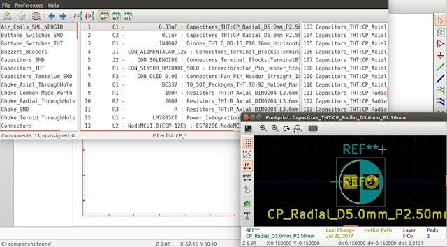
tool. It is not impossible to do this with just one monitor, although it
is a little “messy”. Using only one monitor, an image with a suggested
window layout follows:
 |
| PCB Design |
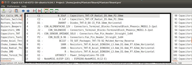
With these two tools open, select component by component in the central part of the footprint association window and choose the most suitable ones for the board. My suggestion is to use the selections seen in the central part of the footprint association window, as highlighted in black in the figure below.
 |
| PCB Design |
Note: it is not necessary
to strictly follow this suggestion, you are free to choose the types of
components you want, but keep in mind that the suggested selection aims at
greater availability of the components on the market and ease of assembly /
welding of the plate.
Once
the association is made, just close the footprint visualization tool, close the
footprint association window.
Netlist
The
last step before we start, in fact, for the design and routing of the PCB is
the generation of the Netlist. In summary, Netlist is a file that
describes all the connections that should exist between the electronic
components of your project, in addition to the relationship between the
components and your chosen footprints. This is something very important,
being the link between the PCB project and the schematic circuit.
To
generate it, follow the procedure below:
- On the
schematic circuit screen, on the toolbar, click on the button with a
drawing with the inscription “Net”, as shown in the following figure:

Circuit board design - A window
will appear. In it, select the option "Default Format" and
click "Generate". This process is also usually quite
cumbersome for KiCAD, so it can take a few seconds depending on the
complexity of your schematic circuit and your computer's settings

Circuit board design - Note,
highlighted in the previous figure, the name of the generated Netlist file
(PlantaIoTBoard.net). It can be seen from your project files on the
main KiCAD screen, as shown in the figure below:

Circuit board design
PCB: component layout
The
time has come to design, in fact, the PCB! For that, we will need to run
the Pcbnew tool . To do this, use the shortcut on
the toolbar on the printed circuit screen, as shown in the following figure:
| PCB |
Pcbnew
will open. The first thing to be done on it is to load the Netlist
generated in the previous topic. To do this, click on the shortcut for
“Read netlist” shown in the figure below.
 |
| Circuit board design process |
On
the screen that appears, click "Browse", select your Netlist file and
click "Read Current Netlist" and then "Close". Reading
the file, as well as other things described here, may take a few seconds
depending on the configuration of your computer and the complexity of your
circuit.
After
reading, the Pcbnew screen will be a little different, containing all the
components of the la circuit, as well as the connections between them. See
the figure below:
 |
| Circuit board design |
You
may have noticed that the components are all “stacked up”. To resolve this
situation and space out the components, there is a feature of KiCAD called
“Global Spread and Place”. To use it, follow the procedure:
- Go to
“View> Switch Canvas to Default”
- Use the
shortcut illustrated in the following figure to enter to enable the “Mode
Footprint”.
- Right-click
on any empty (free of components) on the screen and access the option
“Global Spread and Place”. There, click on “Spread out All
Footprints”. If a dialog box appears, answer ok / yes and you are
done! Your circuit should look similar to the figure below:

Circuit board design - Click on
the shortcut in step 1 again to exit “Mode Footprint”
Note: although this is a
very useful feature to make the circuit more visible, it will not consider the
connection between them in the layout! Therefore, we still have to
reposition them according to our needs and / or connections between components.
Here
comes the “artistic side” of the thing: position the components so that they
can be organized in a way that is easy to assemble (maybe even do with single
layer, if you're lucky!). This is something that does not have much to
explain, except to say that it must be done with common sense and always aiming
at the best possible assembly (by "best assembly", understand the
simplest, after all who will assemble / weld the sign when ready is you).
This
is also the longest step: depending on your experience and “spatial view” of
the circuit, it can take hours (maybe days), but don't be discouraged: it is a
valuable experience for the future.
In my case, I found that the most suitable layout (aiming for a single layer
board and simple to assemble) is the one shown below:
 |
PCB: board routing
It
is time for card routing. The routing consists of connecting the
components with the tracks of the printed circuit, in the desired
configurations (thickness, diameter of the hole and its metallization, distance
between tracks and the rest of the circuit, etc.). For beginners, printed
circuit tracks are analogous to wires connecting component terminals.
There
are two routing options: automatic and manual. The automatic is not
recommended (especially for those who are starting in this area) because, in
addition to doing a job that will need to be understood by you, it leaves a lot
to be desired regarding the use of the layer (in short, it is “waste” in making
trails and use layers, which means more expensive PCBs to manufacture and
inefficient in space utilization). For these reasons, we will do manual
routing in this article.
To
do this, do the following:
- Select the
bottom layer, as shown in the figure below.
Note: The name B. Cu means:
B: Background Layer
Cu: Layer with Copper / conductive surface. - That done,
it means that every routing we do will be applied to the selected Layer
(in this case, lower). To make a track, in the right sidebar of
Pcbnew, click on “Add tracks and routes”, as shown in the figure below:
- Choose a
Pad ("circle" around the component terminal) and click once with
the left button. Drag the mouse to the target pad and double-click
with the left button. There, you made your first track! It will
be as shown in the figure below:

Circuit board design - Now repeat
the procedure for all the tracks to be done. Here, again, it is
something that requires a more “artistic” side, because you should try, at
all costs, to put all the tracks on this layer. Remembering that a
track can NEVER pass over another one on the same Layer!
This is something that can take a lot of time (and patience), but you must go through this experience (it is valuable for future projects). Below is the routing that I found most convenient (and that can be done in a single layer):
 |
| Circuit board design |
PCB: defining the plate area and ground
plane
Now,
it will be necessary to define the area of the plate, that is, of the entire
area available for the project, select which is really relevant / should
constitute your plate. In addition, the ground plan will be defined, which
consists of filling all unused space by the trails with a ground conducting
plan. The purpose of the ground plane is to serve as a protection against
electromagnetic noises that fall / are irradiated on the plate. These
noises, if impacted on the plate, will be more likely to be directed to the
ground planes than to the circuit tracks, not harming the signal that travels
through them. If the ground plan is not made, the noises will directly impact
the trails, impairing (and, often, making unfeasible) the correct functioning
of the circuit.
To
define the area of your plate and the land plane, do the following:
- In the
toolbar on the right, select the option “Add filed zones”, as shown in the
figure

Circuit board design - Left-click
where you want to be one of the vertices of the plate. A window will
appear, asking for details of the plan that will be created. There,
select the GNDREF option and click OK. See the figure below:

Circuit board design - Now,
clicking with the left button to define the vertices of the plate, go
through the entire plate, forming a rectangle. At the last vertex,
double-click the area to be closed.
Tip: do not make the rectangle too close to the components, this can increase the chances of PCB manufacturing errors. - Click on
“Perform PCB Rules Check”, as shown below

Circuit board design - A window
will appear. Click on “Start DRC” and then on Ok.
Important: this step will check your PCB for errors. If any arise, correct them immediately. - Once this
is done, your plate will be routed, with a defined area and with a ground
plane, as shown in the figure below:

Circuit board design
3D preview of your board
For
your delight, you can have a 3D preview of your board in KiCAD! To do this,
on Pcbnew, go to “View> 3D Viewer”. Notice how the board looks in 3D:
 |
| Circuit board design |
And to have the plate manufactured, how do
I do it?
The
PCB project has come to an end, but what about making the board? How is
done?
For
this, one of the most popular ways is to use Gerber Files. The Gerber
Files are files generated by your PCB design program that show the manufacturer
how each detail of the board should be done, so in possession of these files
the manufacturer can manufacture the boards exactly as specified.
To
generate your card's Gerber Files, follow the procedure:
- On Pcbnew,
click on Plot, as shown below

Circuit board design - On the
screen that appears, leave it as shown in the figure below

PCB Design - Click on
“Browse” and define a directory where the generated files will be
saved. If you prefer, create a sub-directory within your project's
directory, for greater organization.
- Click on
“Plot”
- Then,
click on “Generate Drill File”, leave it as shown in the figure below,
place the same output directory as in step 4 and click on “Drill File”.
Okay, everything you need to have your PCB manufactured is in the directory you chose!
 |
| Circuit board design |
Now
all you have to do is send the Gerber Files and Drill Files to the manufacturer
and request a quote (and manufacturing, if the budget pleases you, of course).



No comments
Note: Only a member of this blog may post a comment.